X-Ray Vision: Berkeley’s High-Speed Electrons Fuel Atomic-Scale Science

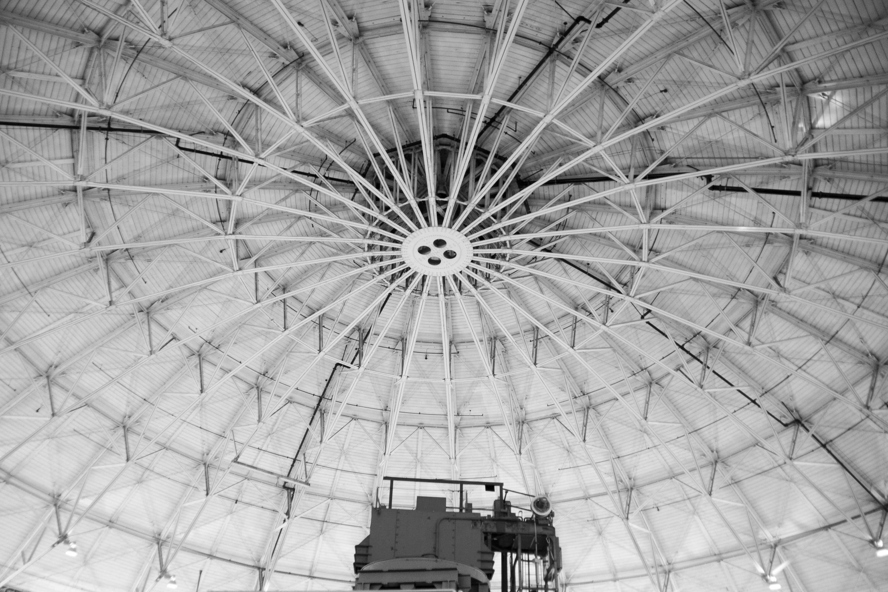
The same dome that housed Ernest Lawrence’s 184-inch (4.67-meter) cyclotron now arches over the Advanced Light Source at Lawrence Berkeley National Laboratory.
Text and photos by Amelia Jaycen
BERKELEY, California—A group of eager writers attending the World Conference of Science Journalists 2017 stood on an upper platform at Berkeley’s Advanced Light Source (ALS) research lab. Under their feet, electrons raced at nearly the speed of light. Overhead, an iconic domed ceiling—the same ceiling under which Nobel laureate and nuclear scientist Ernest Lawrence invented the cyclotron—endowed a jumbled space full of laboratory pipes and instruments with the airy feel of a giant atrium.
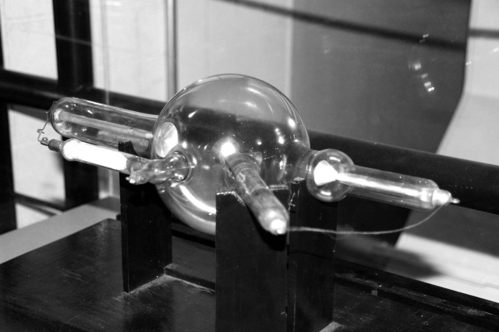
An X-ray tube from 1923 is a testament to the history and development of ALS, one of the world’s brightest sources of soft X-rays.
As the journalists enjoyed their visit to Lawrence Berkeley National Laboratory on 29 October, magnets steered groups of electrons around a giant circle, 200 meters in circumference, and released light at 40 different openings. “Think of the electrons as cars with their headlights on,” said physicist Roger Falcone, director of ALS. “As they drive around, flashes of light come out each of those ports.”
Peering into molecules
At the ends of each of the 40 light beams—in a range of wavelengths spanning the electromagnetic spectrum from infrared to both soft and hard X-rays—instruments perform experiments that depend on this constant flow of electrons. The relentless light penetrates materials and allows scientists to study the atoms and molecules inside. Each beam can be tuned to a different wavelength to reveal a particular element or molecule. Scientists use the beams to study everything from how the crystallographic structure of a new polymer reflects light rays to how a bacterium breathes in the absence of oxygen.
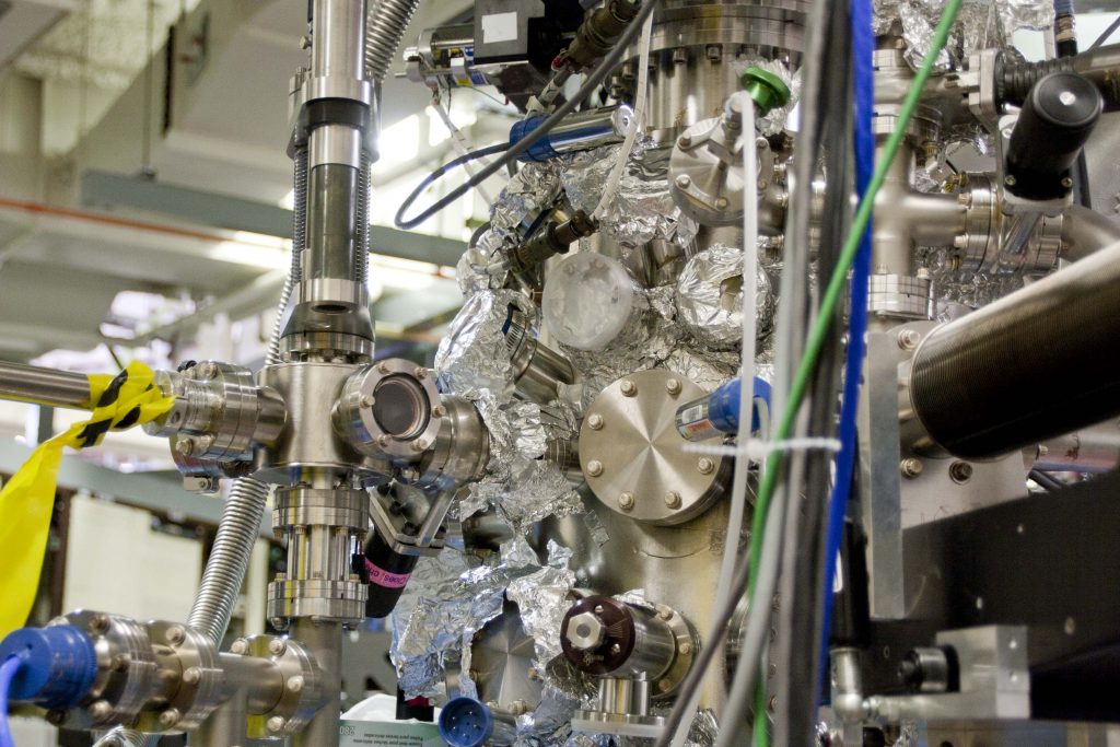
Detectors at ALS are covered in tin foil as part of a cleaning process using extremely high temperatures to bake away impurities.
Nanoscience is all about trying to understand how individual atoms work. It’s the science of the absurdly small, said Branden Brough, deputy director of Berkeley Lab’s Molecular Foundry.
A firehose of nano-information
As tiny the scale of nanoscience is, the field generates huge amounts of data.
A typical experiment at ALS can produce hundreds of terabytes of data. The nearby National Energy Research Scientific Computing Center (NERSC), home of the world’s sixth-fastest supercomputer, processes the firehose of data coming from ALS. The NERSC supercomputer operates at 31 petaflops, can run 30 trillion calculations a second, and includes the world’s fastest network for science, ESnet—a 100-gigabit network spanning the Atlantic Ocean to transfer data in and out of the CERN particle physics laboratory in Geneva, Switzerland.
Berkeley Lab researchers have pioneered algorithms that make computer modeling better able to solve big problems. For example, an advance called “adaptive mesh refinement” allows computers to provide higher resolution in areas of high interest, while peripheral areas remain at low resolution.
Mathematical theory and modeling can help make computations simpler. At the Molecular Foundry, Berkeley Lab scientists are inventing non-natural building blocks—synthetic molecules—that can self-assemble into artificial proteins. These could yield industrial catalysts or therapeutics that don’t require refrigeration.
But since researchers are working with materials that have never existed before, the process is a giant game of trial and error. For instance, a single experiment building a polymer with a chain of 50 molecules could have 200 to the 50th power possible sequences—far too many to synthesize.
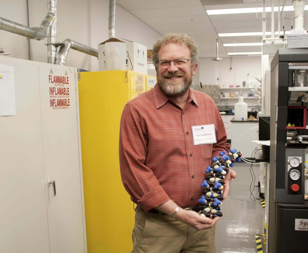
Ron Zuckermann of the Molecular Foundry designed robotic instruments to mix chemicals that self-assemble into synthetic molecules.
“We desperately need theory. We need guidance. We need an understanding of the tricks biology uses to make a catalyst, an enzyme,” said Ron Zuckermann, director of the biological nanostructures facility. If researchers knew nature’s tricks for building molecules, he said, they could then build the same features into synthetic molecules. “You can’t beat an antibody or an enzyme for just sheer beauty or functionality… We call it bio-inspired design, or bio-mimetic architecture,” Zuckermann said.
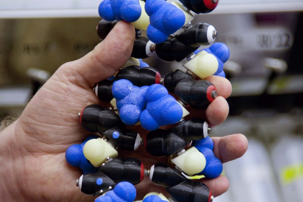
Colored magnets simulate the cooperative binding interactions of hydrogren as a model for building materials that are similarly structured but completely synthetic.
Next door, at the National Center for Electron Microscopy, scientists can image these new materials at atomic-scale resolution and measure molecular bonds to a precision of one picometer—one one-hundredth of an Ångström. That’s small enough see relationships between individual atoms and sharp enough to expose a lot of the information locked inside nanoparticles.
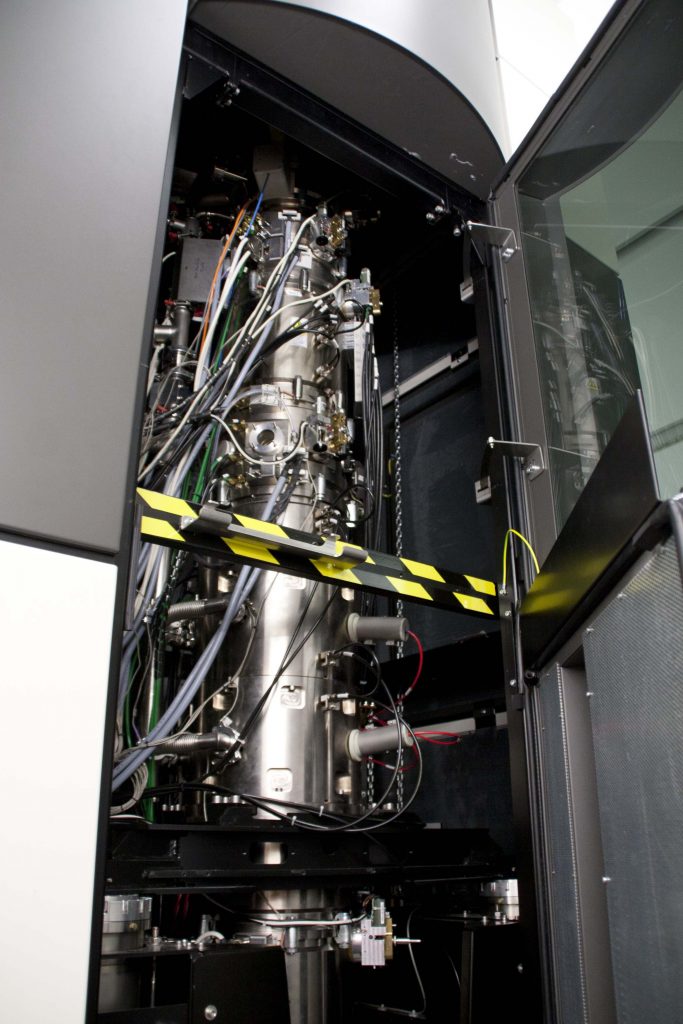
This transmission electron microscope uses 200 lenses and aberration correction to achieve atomic-scale resolution with picometer precision.
One rule to bind them all: Collaboration
Nanotechnology may be the science of the absurdly small, but it’s also a science that is inherently multidisciplinary, said Brough.
To earn a spot at Berkeley Lab and access to its experts and facilities, a scientist must show two things: a really good idea and a driving need for interdisciplinary collaboration. That draws thousands of researchers each year, Brough said: Intense cross-disciplinary collaboration is “a really cool model” for doing science.
—
Amelia Jaycen is a science journalist launching a career covering physics, energy, materials and engineering. Most of all, she’s interested in the stories electrons tell. She recently earned her master’s degree in journalism and now writes about ocean technology on the east coast of the U.S. Reach her at ameliajaycen@gmail.com.